HP5065A Working Digital Clock
As I detailed last month, the LED clock in my HP5065A was not a happy camper and while investigating that I realized just how much of my HP5065A was only there to drive the clock.
So I decided to jump into KICAD and design a PCB to replace the sick parts of my LED clock, and make the divider-chain before it surplus to requirements.
Turned out quite nice I think:
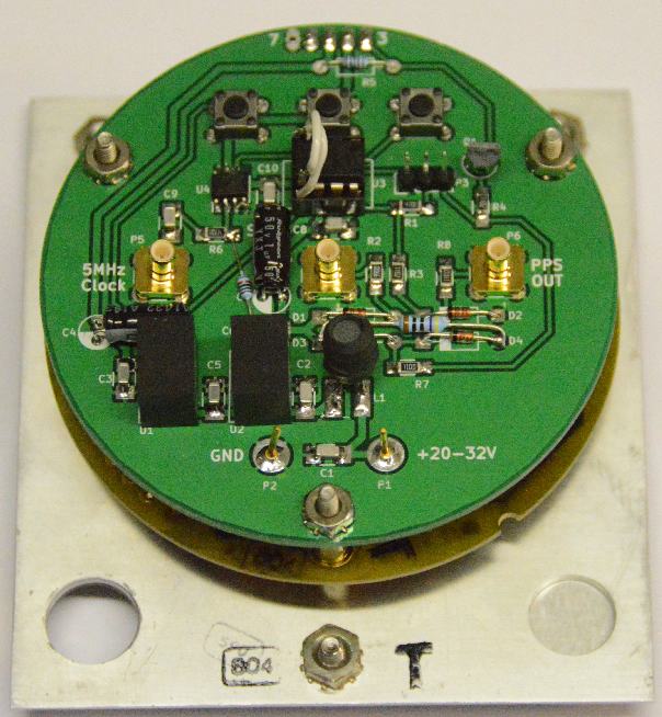
I used the SeeedStudio PCB service, and that cost me about $59 (including shipping) for 10 PCBs.
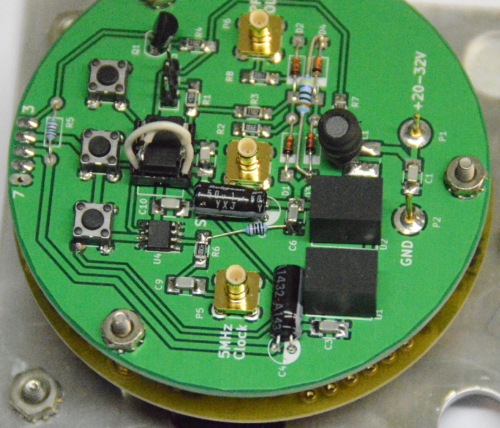
As always there are things you only discover once you get everything hooked up in my case two bleed-resistors:
Almost but not quite
The 470R across the diodes are to bleed the 3.3V supply when you power off, otherwise the supply tends to linger at 0.9V forever, which is just enough to keep the LPC810 processor in some kind of hibernating state, from where it does not do a RESET when you reapply power.
Since I’m disabling the normal way to access the “bootloader” in the chip, being able to do a proper power-cycle to go through my code to get there - at least when you hack the software.
The 10k nearest the camera is to bleed the comparator input to GND in case there is a transient - same story, takes forever without it.
The two white wires on the LPC810 itself is to swap pins 4 and 5 after changing my mind about it after sending the Gerbers of to SeeedStudio.
I explained this foobar last month, but the short summary of it is that unless you swap the pins, the PPS-OUT has 33⅓ nanosecond jitter relative to the 5 MHz output.
Back then I decided to take the shortcut, but after getting the short-cut way to work, I spent an hour more on the firmware to make it autodetect if you swapped the pins and do the right thing.
Fat Fingers Need Not Apply
What I hadn’t fully appreciated is just how tight the mounting space for the clock is. There must be some trick to umounting it, but I havn’t found it. Maybe one simply has to unmount the entire front panel ?
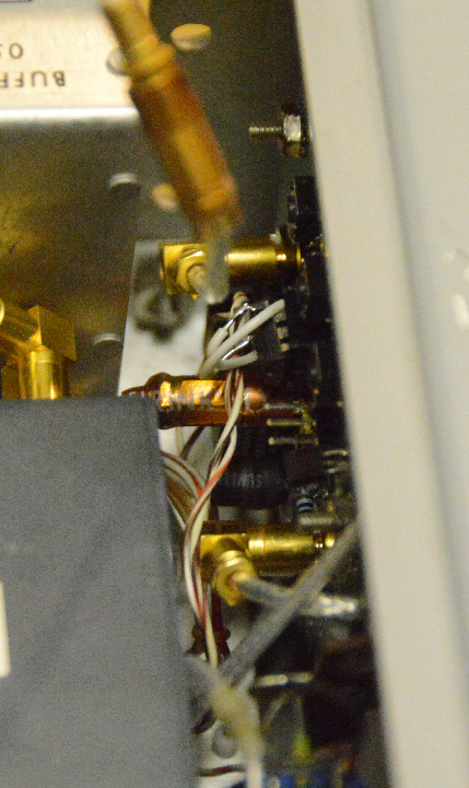
The most important lesson learned for anybody who want to replicate this project (Drop me an email, I have 9 spare PCBs) is to use a right angle SMB connector for the 5MHz clock input.
By using 6 mm distance-pipes between the two PCBs, you can just exactly get away with a vertical SMB for the 5MHz clock, but finding a low profile connector for the PCBs is tricky. (Of course you can just solder a wire between the boards…)
Other than that, it’s just a very tight space, but it can fit and the cables can be made to work.
5 MHz comes from the OCXO, one of the SMB-SMB cables from the assembles removed is perfect, if you use a right angle connector.
PPS-IN comes directly from the SYNC connector on the back-side. This is probably the tightest fit.
PPS-OUT goes to the front panel connector on the clock-assembly and the cable is 25cm longer than necessary. I coiled it up between the Buffer amplifier and the chassis.
Power comes from the same place as previous directly from A2-8, and GND from the solder-lug on the chassis under the clock.
Firmware
First thing, the watchdog timer is configured, it will reset the LPC810 if things don’t happen as planned.
Next 86400 pulses are sent to the display, that takes a couple of seconds.
If the “Minute” button is pressed during this sequence the LPC810’s builtin bootloader is entered, it can be accessed with 3.3V async via the G|R|T connector.
Then the frequency of signals on pin 4 and 5 are measured, and whichever one looks most like a 5 MHz clock-signal is chosen, and things configured accordingly.
At this point approx 10 pulses a second are sent to the display to indicate that the clock has not been set.
Pressing any of “Hour”, “Minue” or “Second” shortly will send respectively 3600, 60 or 1 extra pulses to the display, in addition to the 1 Hz pulses.
If the Second button is held down for longer than a second, the 1Hz pulses stops until the button is released again or a low to high flank on PPS-IN.
Recommended procedure:
Sync to external 1 PPS (From a GPS maybe ?)
Step seconds to correct value
Step minutes to correct value
Step hours to correct value
To Let
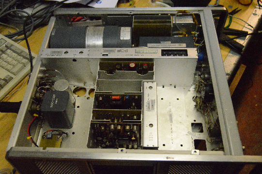
And the final result, a lot of empty space and a few Watts lower power-drain.
As so often I forgot to do proper before/after measurements, but the new clock-electronics uses exactly 1 Watt of power which is less than the old clock-electronics, and on top of that I have eliminated:
A4 100 kHz Frequency Divider
A5 1 Hz Digital Divider
A6 1 MHz Frequency Divider
A16 Digital Divider Power Supply
I have published the firmware and PCB files on github.
phk